
SAMPLE CODE
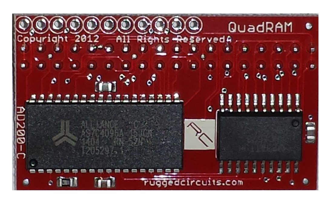
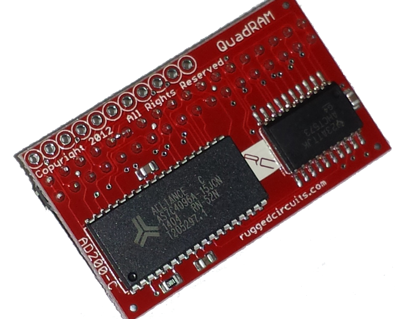
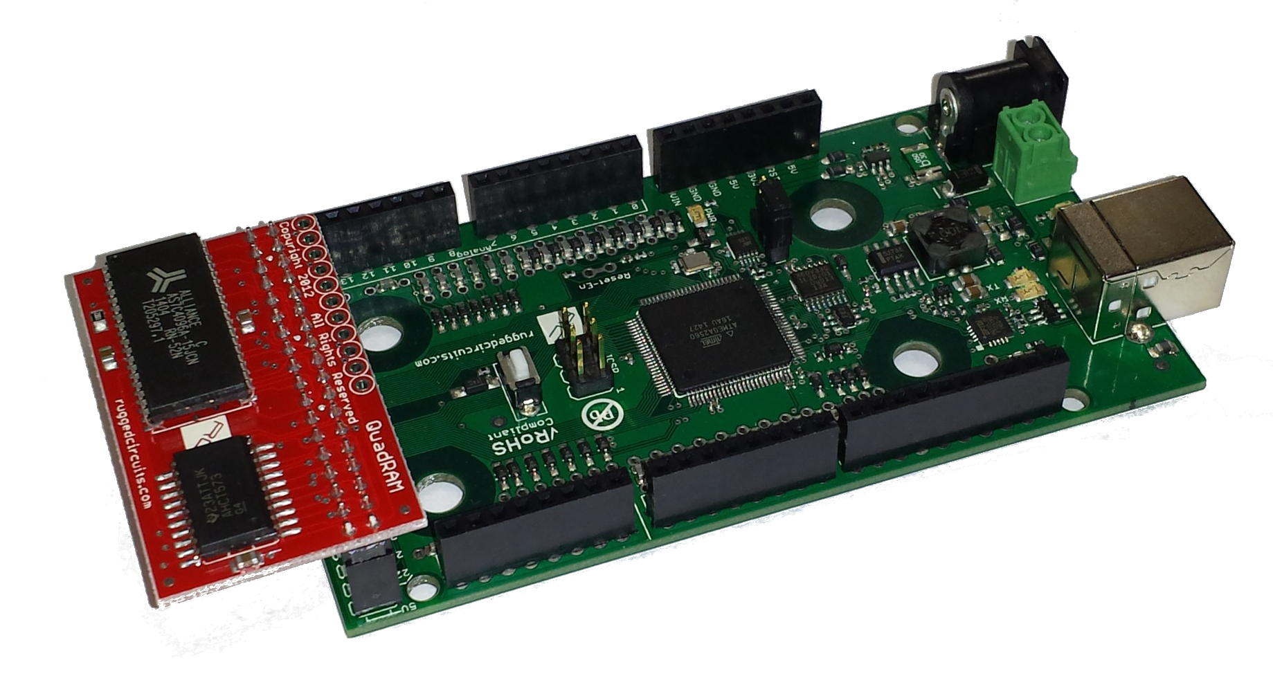
Here are some sample sketches that illustrate different ways to use the 512 kilobytes of RAM on the QuadRAM Shield,
RAM Test
This sketch shows how to test the QuadRAM shield. It demonstrates how to use the bank control and high memory masking to access the full 512 kilobytes of external RAM.
Download: RAMTest.pde
Simple Code
This sketch demonstrates the simplest way to access the external RAM, with no bank control, to access ~56 kilobytes of external RAM. The sketch computes a 16384-point complex FFT of a test sinusoid.
Download: RAMDemo1.zip
Dynamic Memory Allocation
This library is a port of Andy Brown's xmem library to the QuadRAM shield. It allows you to use the dynamic memory allocation functions (e.g.,malloc, free) to allocate memory from the 512 kilobytes available on the QuadRAM shield.
Download: xmem library Version 1.2
Usage
Enabling the External Memory Interface
Most of the pins used for accessing external RAM are automatically taken care of by the microcontroller. In order to enable the memory interface, the SRE bit in the XMCRA (External Memory Control Register A) has to be set: XMCRA = _BV(SRE);
The external RAM on the QuadRAM is fast enough to support zero-wait-state operation so all other bits in the XMCRA register can be set to 0.
Enabling the External RAM Device
The actual RAM device itself has to be enabled by setting PD7 (Arduino digital pin D38) low: pinMode(38, OUTPUT); digitalWrite(38, LOW);
If this pin is set to HIGH then the expansion header pins can be used for other purposes and external RAM will be disabled.
Reserved Pins
When external RAM is enabled, pins PA0-PA7 (digital pins D22 through D29), PC0-PC7 (digital pins D30 through D37), PG0-PG2 (digital pins D39 through D41), PL5-PL7 (digital pins D44 through D42) and PD7 (digital pin D38) are reserved for the external memory interface.
Bank Selection
Pins PL5 through PL7 (digital pins D44 through D42) are used to select between eight 64 kilobyte RAM banks, which together form the 512 kilobyte external RAM. The usage of these pins is described below in the RAM Access Options section below.
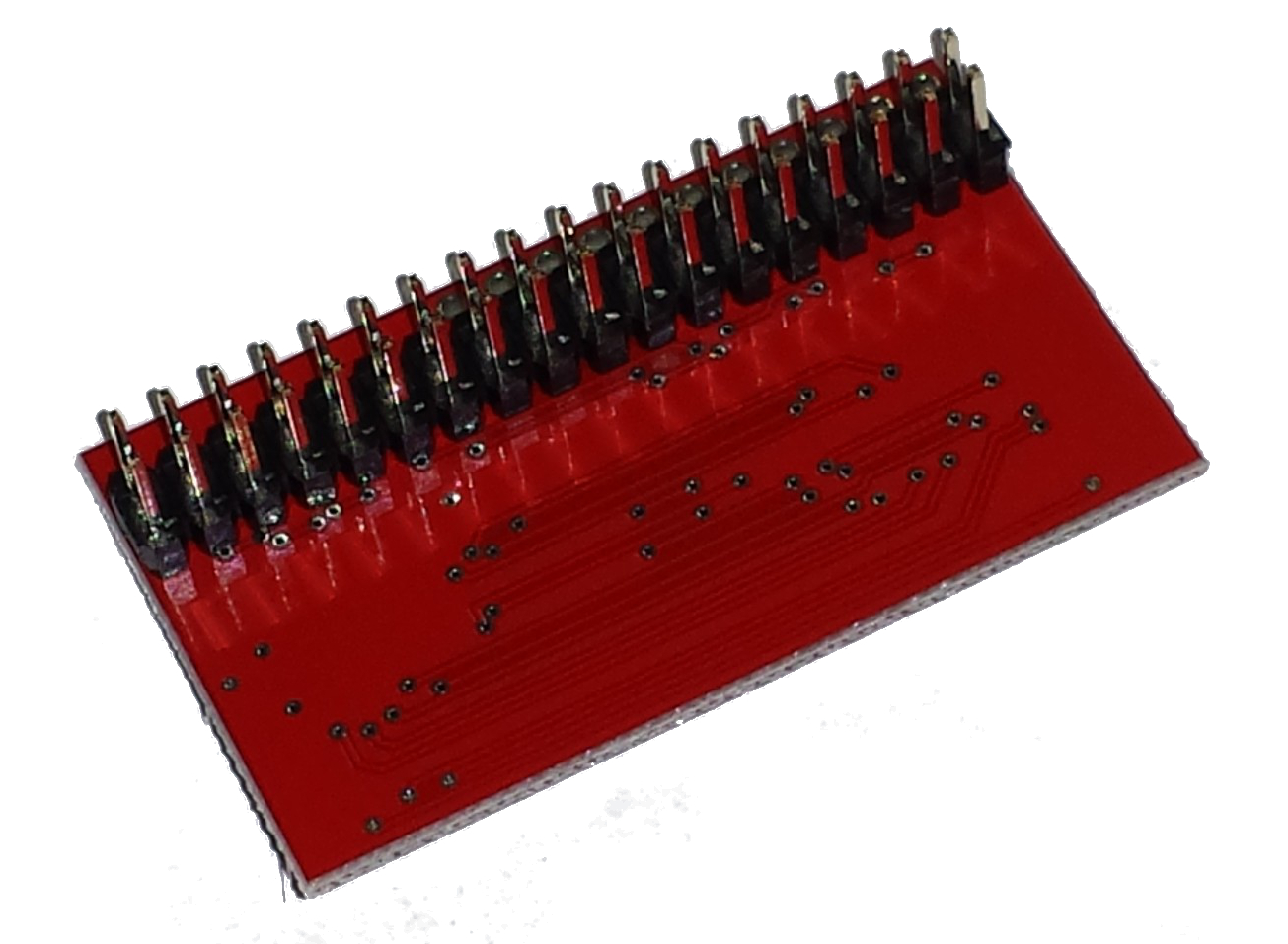
Expansion Pins
Unused pins from the expansion connector are brought out to pads on 0.1" centers for easy interfacing. The picture below shows which pins are brought out and their positions on the QuadRAM shield.

RAM Access Options
The QuadRAM shield provides 512 kilobytes of external RAM, but the ATmega 1280/2560 address bus is only 16 bits wide, meaning the microcontroller can only access 64 kilobytes of RAM at a time. Furthermore, part of the 64 kilobyte address space is used by the ATmega 1280/2560 processor for internal registers and the 8 kilobytes of internal RAM. In this section we look at the details of how to work with these limitations of the microcontroller.
Simplest Approach-- 56 kilobytes
The simplest approach to using the QuadRAM is to do nothing. Here is the memory map of the ATmega 1280/2560 processor showing the locations of the internal registers, internal RAM, and external RAM (the memory map is figure 8-2 from the Atmel ATmega1280/2560 data sheet).
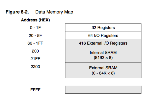
Memory from the addresses 0x0200 through 0x21FF is the normal 8 kilobytes of internal SRAM. Memory from locations 0x2200 through 0xFFFF (56832 bytes) is external SRAM provided by the QuadRAM shield. Therefore, if all you need is ~56 kilobytes of RAM, just start accessing memory at memory location 0x2200 and higher. Here is an example that shows how to fill this 56 kilobyte region with an increasing sequence of 8-bit numbers:

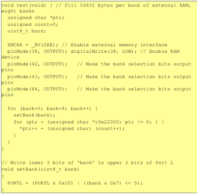
Bank Control -- 444 kilobytes
If you want to access more than ~56 kilobytes of RAM, you will have to get around the microcontroller's limited 64 kilobyte address space. The actual RAM device has a 19-bit address bus -- the 17th through 19th bits are provided by the microcontroller pins PL5, PL6, and PL7 (digital pins D44, D43, and D42) while the lower 16 bits come from the microprocessor itself. This means by setting pins D42-D44 high and low, you can switch between eight totally separate 64 kilobyte banks of RAM. In each bank, ~56 kilobytes (56832 bytes) is directly visible starting at address 0x2200, just like before. This means that by controlling D42-D44 we have access to 8 banks of RAM, with 56832 bytes in each bank, for a total of 454656 bytes (or about 444 kilobytes) of RAM.
Here is the same code example from above, which fills all 56832-byte banks with numbers:
In summary, accessing ~444 kilobytes of the available 512 kilobytes on the QuadRAM shield is fairly straightforward. To get at that last 68 kilobytes is going to take a bit more work.
High Memory Mask -- 512 kilobytes
The reason we can't easily access that last 68 kilobytes is because the address range from 0x0000 to 0x21FF is reserved for the microcontroller's internal registers and internal RAM. The way to work around this limitation is to use a feature called high memory masking (see section 9.4.2 of the Atmel ATmega1280/2560 datasheet which describes the XMCRB register). The principle is similar to the bank selection mechanism above, except now we use four bank select pins to select between sixteen 32 kilobyte memory banks. These sixteen 32 kilobyte memory banks represent the entire 512 kilobyte external RAM.
Normally, all the pins in Port C (PC0 through PC7) are driven by the external memory interface whenever an external memory access occurs. PC7 is connected to address bit 16 (and PL5 through PL7, the bank selection bits, are connected to address bits 17 through 19). This means that by controlling both PL5-PL7 and PC7 (instead of letting PC7 be driven by the microcontroller), we can control access to one of sixteen 32 kilobyte banks, each of which uses address lines 1 through 15. The XMCRB register lets us do this; by setting the XMM0 bit in XMCRB to 1, PC7 is "released" by the microcontroller and becomes a normal digital port pin. We still have the problem that memory accesses in the range 0x0000 through 0x21FF are used for internal registers and memory, and do not cause external memory accesses. This problem is easily fixed: always generate memory accesses at address 0x8000 and above. The memory range from 0x8000 through 0xFFFF represents a 32 kilobyte memory bank. The choice of bank is controlled by controlling pins PC7 and PL5-PL7.
The code that shows full access to the 512 kilobyte RAM on the QuadRAM shield is shown below.

For a more practical example, see our memory test sketch (RAMTest.pde) to see how this high memory mask approach is used.
FAQ- Frequently Asked Questions
Q-How would one rate the level of difficulty for integrating the QuadRAM?
A-The QuadRAM will require some higher level of programming and experience using Arduino.
Q-I am having difficulty writing code for the QuadRAM. Would Rugged Circuits review my code for implementation?
A- We do not review or verify any code. We have created the above sketch examples for your personal review to help guide you along.
Q-I have reviewed the above sketches but I am still having difficulty with my code which is causing corruption and crashes. Most of the FFT is code that has nothing to do with memory access, and both RAMDemo1 and RAMTest use dynamically-assigned pointers. I have no idea why these are Processing .pde apps and not Arduino .ino apps…
I want to be able to assign a static array such as:
float fa[4000];
A-One must define his variable like this...
float* fa = (float*)0x2200; // up to 56kB or 14208 floats (4 bytes each)
instead of
float fa[1900]; // <- This places the variable on the stack which isn't large enough and crashes the system.
The key here is that the compiler / environment doesn't know the memory is there so you have to access it manually with pointers as the example shows.
We would create a structure with all of the variables we wanted to place in the extra memory and then use that to access them since that makes them easier to keep straight.
Otherwise in this example a user is trying to allocate the memory on the stack (local variable) and the stack isn't that large, causing memory corruption. While there is extra sram, the compiler doesn't know it's there, and even if it did the stack wouldn't by default be large enough. The example on the Rugged Circuits site explains how to use the memory.